Terahertz waves: the invisible guardian of semiconductors
15/07/2025
By Professor Israel Arnedo, Director at das-Nano.
At the heart of our digital lives lie semiconductors, special materials used to produce the tiny components that power everything from smartphones to electric vehicles, commonly referred to as chips.
Manufacturing these chips is an incredibly complex process that requires almost unimaginable levels of precision. This is where terahertz wave inspection technology is beginning to play a key role, helping to ensure that these devices function as intended while also reducing the environmental impact of their production by detecting any faults as early as possible in the complex manufacturing chain.
The importance of inspection in semiconductor manufacturing
Chip manufacturing involves multiple stages of material deposition and etching, including metals, semiconductors and insulators. The integrity of each of these layers and their electrical properties must meet strict quality standards, as even a minimal deviation from the design can result in failures in the final devices; failures that would only be detected during final testing, leading to costly and environmentally damaging waste.
Traditional inspection methods have worked well, but they face limitations in their ability to analyse complex materials non-destructively and at high speed. This has opened the door to new solutions, such as terahertz waves.
What are terahertz waves and why do they matter?
Terahertz waves, located between microwave and infrared radiation on the electromagnetic spectrum, have a unique capability: they can penetrate many materials and analyse their electrical properties without damaging them. This technology makes it possible to inspect and measure ultra-thin layers quickly and accurately, which is essential in semiconductor production.
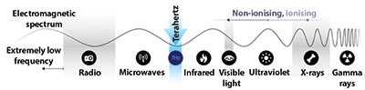 | ||
| On the electromagnetic spectrum, terahertz waves are located between microwave and infrared radiation |
The key advantages of terahertz inspection include:
- Non-destructive measurement: terahertz waves allow for the analysis of ultra-delicate materials without altering them, enabling 100% inspection of production output;
- They can differentiate between multiple material layers, providing detailed data on thickness and uniformity; and
- When integrated into production lines, this technology shortens inspection times and allows real-time adjustments, helping avoid costly reprocessing.
Impact beyond precision
In addition to ensuring the quality of the final product, terahertz wave inspection also has a significant impact on sustainability. This technology enables the detection of not only defects but also inhomogeneities and variations in the electrical properties of materials, allowing for more precise process control. By optimising the use of materials and energy, it contributes to reducing waste and improving efficiency, an essential factor in an industry that is facing growing global demand while being under increasing pressure to operate more responsibly.
The future of chips and terahertz
The adoption of advanced technologies such as terahertz waves is transforming chip manufacturing, not only from a technical standpoint but also strategically. In a global context, where demand for these components continues to grow exponentially, ensuring their quality efficiently and sustainably is no longer optional, it is essential.
At das-Nano, it is believed that terahertz waves are more than just an inspection tool: they are a key element in driving the chip industry towards a future where new materials enable smarter, more environmentally friendly designs.