Non-contact charge carrier density mapping of SiC semiconductors
12/12/2025
As semiconductor devices become smaller, faster and more powerful, accurate knowledge of material properties such as charge carrier concentration and mobility becomes critical. In particular, the dopant concentrations in both the bulk substrate and thin epitaxial layers are key parameters, which ultimately determine the performance and reliability of power devices used in electric vehicles, renewable energy systems and high-voltage electronics.Traditional analysis methods such as mercury capacitance-voltage (mCV) or four-point probe techniques require physical contact with the sample. They are slow, often destructive and susceptible to contamination, an issue that is especially problematic for high-purity materials such as silicon carbide (SiC) or gallium nitride (GaN).
In contrast, terahertz time-domain spectroscopy (THz-TDS) enables contact-free, fast and spatially resolved measurements of charge carrier density and mobility directly on wafers, without any electrodes or surface preparation.
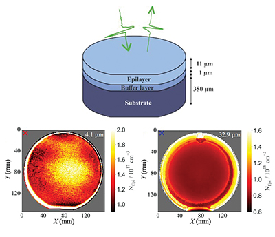 | ||
| Sample geometry (top image) and charge carrier concentration mappings of two epilayers of different thickness (bottom images)[1] |
In a collaboration between Fraunhofer Institute for Industrial Mathematics (ITWM), Fraunhofer Institute for Integrated Systems and Device Technology (IISB), Technical University Freiberg, Freiberg Instruments and Toptica Photonics, carrier concentrations of epilayers and their bulk substrates were determined simultaneously.
An entire SiC wafer was mapped in under 70 min with more than 17,000 data points, compared to 20 min for only 25 points using mCV. The results demonstrated a good agreement between THz-derived carrier densities and mCV reference measurements. THz-TDS measurements successfully analysed doping concentrations that varied over three orders of magnitude and characterised epilayers as thin as 4 µm. In addition, the mapping identified inhomogeneities and defect distribution over the wafer area.
In summary, the transition to SiC and other wide-bandgap semiconductors demands new metrology tools that match the complexity of the material and the production speed. THz-TDS fulfils this need, delivering non-contact, broadband and high-speed measurements of charge carrier concentration and wafer uniformity.
Reference
1. J Hennig et al, ‘Simultaneous charge carrier density mapping of SiC epilayers and substrates with terahertz time-domain spectroscopy’, Optics Express, Vol 33, No 22, pp 45828-45842, 2025.